Professional Team
Our company has a strong R&D and production management team, equipped with advanced production machinery and highly precise testing instruments.
Multiple Business Products
The company operates a series of products including automotive components,3C (Computer, Communication, Consumer Electronics) product casings etc.
High Professional Level
Vietnam Atlantic Industrial Co., Ltd. is a company that integrates research and development, design, production, processing, and sales.
Quality Control Measures
The factory is equipped with comprehensive inspection equipment including CCD inspection equipment, 2.5D microscope, 3D etc.
Product Applications Cover a Wide Range
Including automotive, smartphones, tablets, televisions, smart home devices, medical equipment, industrial automation control, etc.
Good Sales
Products are exported to Japan, the United States, Germany, Southeast Asia etc.
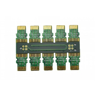
A printed circuit board (PCB) is a structure for assembling electronic components and their connections into a unified circuit that allows electrical current to pass between components. The PCB baseboard is typically made of a rigid nonconductive material, although it can also be built on a flexible base or on a base made up of both rigid and flexible materials. Electronic components such as diodes, inductors and transistors attach to the circuit board, and traces (electrical conduits) connect components.
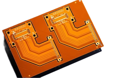
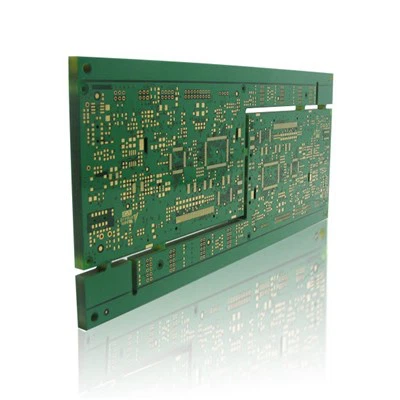

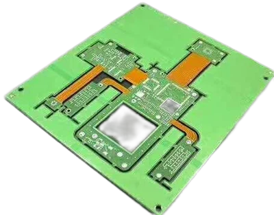
A PCB can be single-layer, double-layer or multilayer. Single-layer PCBs are typically used for simple electronic devices such as home appliances, while multilayer PCBs tend to be built for more complex hardware, such as computer graphics cards and motherboards. Double-layer PCBs allow for greater density than single-layer PCBs and are used for electronic devices such as automotive dashboards or LED lighting, for example.
A PCB’s layer count is commonly based on its number of conductive layers. However, a PCB also includes other types of layers, which are laminated together in alternating patterns of conductive and insulating material. Today’s PCBs always contain the following four types of layers:
• Substrate: This is the base, or core, layer. It is typically a rigid insulating material such as FR-4, a fiberglass/epoxy composite. In some cases, the substrate is a flexible material, usually plastic, which can fold or bend to accommodate space requirements. Flexible substrates can also withstand higher temperatures and other harsh conditions. Some PCBs use a combination of both rigid and flexible substrate materials.
• Conductive: This layer is usually made from a thin sheet of copper. On a single-sided (or single-layer) PCB, there is one conductive layer laminated to the substrate. On a double-sided (or double layer) PCB, there are two conductive layers, one on each side of the substrate. A multilayer PCB alternates between the substrate and conductive layers.
• Solder mask: The conductive layer is covered with a solder mask, a nonconductive material that gives PCBs their green color, although other colors can be used. The solder mask acts as an insulator for the underlying traces that are etched in the conductive material. The solder mask is also applied to the bottom of a single-sided PCB.
• Silkscreen: This layer is simply the labeling that is applied to the PCB after all the other layers have been added. The labeling can include numbers, letters, symbols or other information that indicates the various functions of each connection point. The labeling is usually white, but other colors can be used.
A PCB is made up of a mix of these four types of layers. The mix and its organization varies depending on the PCB’s purpose. A single-layer PCB includes one of each of these four layers. A double-layer PCB includes one substrate, but two of each of the other types of layers. A multilayer PCB will contain a mix of conductive and nonconductive layers, although the exact organization can vary. In some cases, a multilayer PCB might also use prepreg as a layer. Prepreg is a dielectric material that’s sandwiched between two core layers or between core and conductor layers.
PCB components use one of two methods to connect to the board: through-hole or surface-mount. Through-hole components have connecting wires (leads) that plug into holes in the board. The leads are soldered to the other side of the board. Surface-mount components are soldered directly to the same side of the board. Today’s PCBs tend to favor surface-mount components because they require less space and are more efficient, although they’re more difficult to assemble.
The PCB components connect to each other via traces, which facilitate communications between the components. The traces are created from the conductive layer through a process called etching, which removes all the copper from the conductive layer except what is needed for the traces.
A PCB can include a range of components, which vary depending on the board’s purpose. Some of the more common types of components include the following:
• Battery: Provides voltage to the PCB’s circuit, although many PCBs receive their power from external sources.
• Capacitor: Holds electrical charge and then releases it when it is needed in the PCB’s circuit.
• Diode: Ensures that the current flows in only one direction, preventing it from flowing in the wrong direction.
• Inductor: Stores energy in the form of a magnetic field, which can help control the fluctuations in the electric current flowing through the PCB.
• Resistor: Limits or regulates the flow of electric current in the PCB’s circuit by generating resistance to the current’s flow.
• Sensor: Detects input from the physical environment — such as vibration, motion, acceleration or infrared light — and responds to that input by generating a corresponding signal.
• Switch: Switches the current on or off as it passes through the PCB’s circuit.
• Transistor: Amplifies or switches the electronic signal passing through the PCB’s circuit.
Many of today’s PCBs adhere to a high-density interconnect (HDI) design, which incorporates a higher wiring density than traditional PCBs. HDI circuit boards require less space and can accommodate more components. The design also makes it possible to create more compact PCBs, which weigh less and require fewer materials. The HDI design is well-suited for use cases where space is an important factor, such as smartphones, home appliances or medical implants.
Before a printed circuit board can be built, it must be designed. This is accomplished using PCB circuit board design CAD tools. PCB design is broken into two main categories: Schematic capture to create the circuitry connectivity in a diagram and then PCB layout to design the actual physical circuit board.
The first step is to develop the library CAD parts needed for the design. This will include schematic symbols, simulation models, footprints for PCB layout, and step models for 3D printed circuit board display. Once the libraries are ready, the next step is to create the logical representation of the circuitry on a schematic. CAD tools are used to place the symbols on a schematic sheet and then connect them to form the circuitry.
At the same time, circuit simulation is run to verify that the design will work electrically the way it is intended to. Once these tasks are completed, the schematic tools will send their connectivity data over to the layout tools.
On the layout side of PCB design, the schematic connectivity is received and processed as nets that connect two or more component pins. With an outline of the intended board shape on the screen, the layout designer will place the component footprints in the correct locations. Once these components are optimally organized, the next step is to connect the nets to the pins by drawing the traces and planes between the pins. The CAD tools will have design rules built into them that prevent the traces of one net from touching another net as well as governing many other widths and spaces needed for a complete design. Once the routing is complete, the design tools are used again to create manufacturing drawings and the output files that the manufacturer will use to build the board.
The design and manufacturing of a circuit board is a step-by-step process: Schematic creation and simulation, setting up PCB design grids and DRCs, component placement, PCB routing, power planes, and finally assembling the BOM and building the board. The next stage of design will focus on these steps.
Before a printed circuit board can be built, it must be designed. This is accomplished using PCB circuit board design CAD tools. PCB design is broken into two main categories: Schematic capture to create the circuitry connectivity in a diagram and then PCB layout to design the actual physical circuit board.
Before starting the design of the board with the CAD tools, it is necessary to ensure that the library part designs are completed. For the schematic, this means creating logic symbols for the parts that will be implemented; resistors, capacitors, inductors, connectors, and integrated circuits (ICs).
With these parts ready for use, begin by organizing them on schematic sheets within the CAD tools. Once the parts are roughly placed, wires can be drawn that represents the connectivity between the pins of the schematic symbols. These lines are known as nets, and they can represent single nets or groups of nets for memory or data circuits. During the schematic capture, process parts must be moved as needed to create a schematic that is legible and clear.
With parts and nets organized on the schematic, the next step is to verify that the circuit will work the intended way. To verify this, employ circuit simulations in a simulation program with the Integrated Circuit Emphasis tool, otherwise known as SPICE. These tools allow PCB engineers to test the circuits they are designing before building the actual hardware. As such, they can save time and money, making these tools an essential part of the PCB design process.
The design tools that PCB designers use have many different capabilities, including the ability to set up design rules and constraints that will keep distinct nets from overlapping while maintaining the correct amount of distance to different objects. There are multiple additional aids available to the designer, such as design grids that can help to place components and route traces in a neat and orderly manner.
With your design database set up correctly and the network connectivity information imported from the schematic, the physical layout of the circuit board is the next task. The first step is to place the component footprints within the board outline in the CAD system. Each footprint will have the net connections displayed as a “ghost-line” image to show the designer which parts they connect to. Placing these parts for their best performance while being mindful of connectivity, areas of excessive heat and electrical noise, and other physical obstructions such as connectors, cables, and mounting hardware is a task that designers will gain with experience. The demands of the circuit alone are not the only constraining factor: designers must consider placing the components so that they can be best assembled by the manufacturer.
With the components placed (although they can be moved as needed), it is time to connect the nets. This is done by converting the rubber-band net connections into drawn traces and planes. CAD tools contain many features that enable the designer to do this, including some automated routing features that save ample time. Great care must be taken when routing to make sure that the nets are the correct length for the signals they are conducting as well as to ensure they do not cross areas of excessive noise. This can result in cross-talk or other signal integrity problems that may degrade the performance of the built board.
Usually, each active component on the board (ICs and other related components) need to be connected to power and ground nets. This is easily accomplished by flooding areas or layers with solid planes that these components can tap into. But, designing power and ground planes isn’t as simple as it seems. These planes also do the important job of returning the signals that are routed with traces. If the planes have too many holes, cut-outs, or splits, it can cause these return paths to create a lot of noise and degrade the performance of the PCB.
With the component placement, trace routing, and power and ground planes finished, your PCB design is nearly complete. The next step is to run a final rules check on it and set up the different text and markings that will be silk screened on the exterior layers. This will help others find components and label the board with names, dates, and copyright information. At the same time, drawings will need to be output that will be used during manufacturing to both fabricate and assemble the final board. PCB designers will also use their tools to come up with cost estimates for building the board.
At this point, the board is ready to be built, and the first step is to send the output data files to a facility for fabrication. This process includes etching all of the traces and planes onto the different metal layers and compressing them together, producing a bare board that is ready for assembly.
At the assembly facility, the board is loaded with the components it needs and runs through different soldering processes, depending on the type of components being used. Then the board is inspected and tested and the final product is ready to be shipped.
Medical devices: Electronics products are now denser and consume less power than previous generations, making it possible to test new and exciting medical technology. Most medical devices use a high-density PCB, which is used to create the smallest and densest design possible. This helps to alleviate some of the unique constraints involved with developing devices for the medical field due to the necessity of small size and light weight. PCBs have found their way into everything from small devices, such as pacemakers, to much larger devices like X-ray equipment or CAT scan machines.
Industrial machinery: PCBs are commonly used in high-powered industrial machinery. In places where current one-ounce copper PCBs do not fit the requirements, thick copper PCB can be utilized instead. Examples of situations where thicker copper PCBs would be beneficial include motor controllers, high-current battery chargers and industrial load testers.
Lighting: As LED-based lighting solutions catch on in popularity because of their low power consumption and high levels of efficiency, so too does aluminum-backed PCB which is used to make them. These PCBs serve as heat sinks and allow for higher levels of heat transfer than a standard PCB. These same aluminum-backed PCBs form the basis for both high-lumen LED applications and basic lighting solutions.
Automotive and aerospace industries: Both the automotive and aerospace industries make use of flexible PCB, which is designed to withstand the high-vibration environments that are common in both fields. Depending on specifications and design, they can also be very lightweight, which is a necessity when manufacturing parts for transportation industries. They are also able to conform to the tight spaces that might be present in these applications, such as inside instrument panels or behind the instrument gauge on a dashboard.
Vietnam Atlantic Industrial Co., Ltd. is a company that integrates research and development, design, production, processing, and sales Our company has a strong R&D and production management team, equipped with advanced production machinery and highly precise testing instruments.We have earned industry recognition and trust by consistently delivering safe, reliable, and of the highest quality products to our customers.
Our company owns its hardware factory, electronics factory, mechatronics factory, and new energy factory. Additionally, we have a dedicated professional team focused on solving a variety of challenges. We are committed to providing end-to-end services to our customers, offering a comprehensive range of products and solutions.
The company operates a series of products including automotive components,3C (Computer, Communication, Consumer Electronics) product casings,communication equipment enclosures ,LED products, equipment enclosures,smart home products, and machined products.
Q: What is CNC service?
A: CNC service refers to the service provided by using Computer Numerical Control (CNC) technology. This technology controls the movement of machine tools through programming to achieve precise service for various materials.
Q: What are the advantages of CNC service?
A: The advantages of CNC service include high precision, high efficiency, high degree of automation, and service for complex shapes. It can achieve precision service tasks that are difficult to complete with traditional service methods.
Q: What materials are suitable for CNC service?
A: CNC service is suitable for a variety of materials, including metals (such as stainless steel, aluminum alloy, copper, etc.), plastics, wood, composite materials, etc. Different materials require the selection of appropriate tools and service parameters.
Q: What are the main steps of CNC service?
A: The main steps of CNC service include drawing analysis, process planning, programming, program verification, machine tool preparation, first piece trial cutting, formal service and subsequent processing (such as cleaning, inspection, etc.).
Q: How to choose a suitable CNC machine tool?
A: When choosing a CNC machine tool, you need to consider factors such as service requirements (such as materials, size, accuracy, etc.), budget, machine tool reliability and maintenance costs. You can consult a professional machine tool supplier or technician for advice.
Q: What knowledge do you need to master for CNC programming?
A: CNC programming requires programming languages (such as G code, M code), service process knowledge, machine tool operation knowledge, and the use of CAD/CAM software.
Q: How to solve the dimensional deviation problem in CNC service?
A: Dimensional deviation may be caused by a variety of reasons, such as tool wear, reduced machine tool accuracy, program errors, etc. Solutions include checking tool status, calibrating machine tool accuracy, verifying and modifying programs, etc.
Q: How to avoid tool chipping in CNC service?
A: Ways to avoid tool chipping include selecting suitable tool materials, setting cutting parameters reasonably, regularly checking tool wear and replacing them in time, etc.
Q: What is the role of cutting fluid in CNC service?
A: Cutting fluid mainly plays the role of cooling, lubrication, cleaning and rust prevention in CNC service. It helps to reduce cutting temperature, reduce tool wear, and improve service quality.
Q: How to ensure the smoothness of the service surface in CNC service?
A: Methods to ensure the smoothness of the service surface include selecting appropriate tools and cutting parameters, controlling cutting forces, using appropriate cutting fluids, and performing subsequent polishing.
Q: What does daily maintenance of CNC machine tools include?
A: Daily maintenance of CNC machine tools includes cleaning the surface and interior of the machine tool, checking and adjusting the machine tool accuracy, lubricating various machine tool components, checking and replacing worn parts, etc.
Q: What should I do if vibration occurs during CNC service?
A: Vibration during CNC service may be caused by insufficient machine tool rigidity, unstable tool clamping, or improper cutting parameters. Solutions include enhancing machine tool rigidity, adjusting tool clamping methods, or optimizing cutting parameters.
Q: How to determine whether the service accuracy of CNC machine tools is qualified?
A: The service accuracy of CNC machine tools can be determined by measuring parameters such as dimensional accuracy, shape accuracy, and position accuracy of service parts. At the same time, the technical specifications and industry standards of the machine tool can also be referred to.
Q: How to choose a suitable coolant in CNC service?
A: Centering operation is an important step in CNC service, which is used to determine the exact position of the workpiece on the machine tool. Centering operation is usually performed using tools such as centering rods or laser centering instruments.
Q: What are the precautions for tool setting operation in CNC service?
A: Tool setting operation is one of the key links in CNC service. Precautions include ensuring that the tool is firmly clamped, the tool setting point is reasonably selected, and collisions are avoided during tool setting.
Q: What is the importance of program verification in CNC service?
A: Program verification is an indispensable step in CNC service. It can help discover and correct errors and unreasonableness in the program, thereby avoiding unexpected situations and losses during the service process.
Q: What is the significance of the first trial cutting in CNC service?
A: The first trial cutting is an important task in CNC service. It can help verify the correctness of the program and the service capability of the machine tool, and ensure the smooth progress of subsequent batch services.
Q: What are the basic knowledge of CNC service?
A: Computer numerical control (CNC) is a manufacturing method that automates the control, movement, and precision of machine tools by using pre-programmed computer software embedded in the tool. CNC is commonly used to machine metal and plastic parts.
Q: What are the rules for CNC service?
A: Never wear gloves when operating a CNC machine. Never wear jewelry or loose clothing. Never try to reach inside a machine while it is running. Never place your hands anywhere near the spindle while it is spinning.
We’re professional cnc services manufacturers and suppliers in China, specialized in providing high quality customized service. We warmly welcome you to wholesale cnc services made in Southeast Asia here from our factory. For quotation, contact us now.

If there are any quality issues with the product or if maintenance are needed, we will provide you with timely after-sales maintenance service to ensure that the issues are promptly solved.
Sign up to receive the latest information from us